

26/7.2018
Infrared (IR) radiation is characterized by a wavelength range from 0.750- 1,000 nm.Due to the limitation of the range of the detector, infrared radiation is usually divided into three smaller regions: 0.750-3 suntan m, 3-30 suntan m and 30-1000 suntan m-- defined as near infrared (NIR), mid-wave infrared (MWIR) and far-infrared (far-infrared) infrared (FIR).Infrared products are widely used in various applications,
More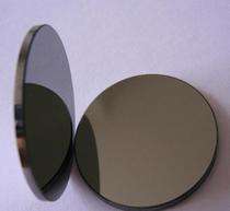
26/7.2018
Germanium wafers have semiconductor properties.It plays an important role in the development of solid physics and solid electronics.Ge melt density of 5.32 g/cm 3, germanium possibility as scare metal, germanium stable chemical properties, temperature not with air or water vapor, but during 600 ~ 700 ℃, germanium dioxide generated quickly.With hydrochloric acid, dilute sulfuric acid has no effect.When concentrated su
More26/7.2018
A processing method for ultra-thin single-crystal germanium wafers is characterized by the following steps: first, single crystal germanium wafers with a thickness of less than 0.5 mm are cut from the single crystal germanium rods using a linear cutting equipment;Secondly, the single crystal germanium chip is loaded in...26/7.2018
Germanium monocrystal is the most commonly used and widely used infrared optical material in the world.Among them, the infrared germanium lens contains different amounts of germanium lenses according to different USES.Mi...